Solum 2.2 inch Electronic Shelf Label Teardown
Quick peek inside the EL029F3WRA
In light of the recent news that the OpenEPaperLink firmware has been ported to the nRF52811 series of chips, I decided to take a look inside the Solum EL029F3WRA to see if it was a viable candidate for a project.
As it turns out, it is very similar to the 2.9 inch tags. I hope to soon have a simple CAD model of the ESL which I’ll use to model a basic pogo-pin programming jig for this particular ESL.
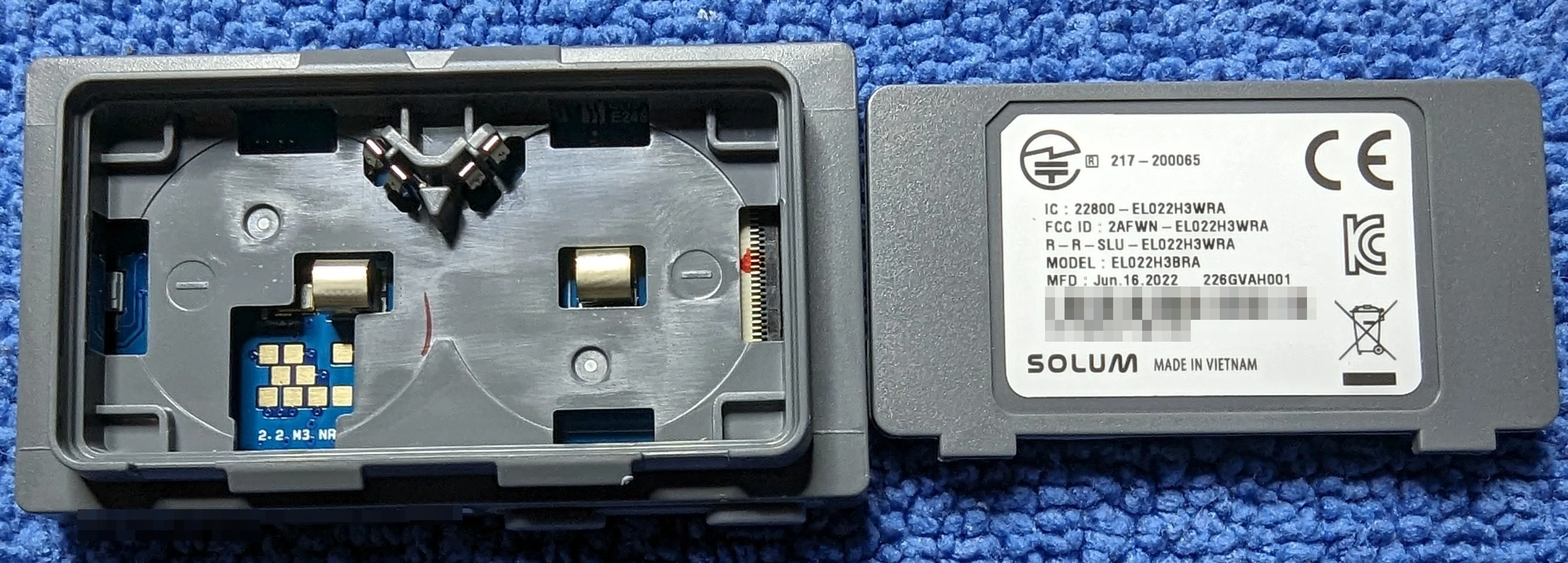
The rear of the ESL is clipped in and can be removed with a plastic spudger.
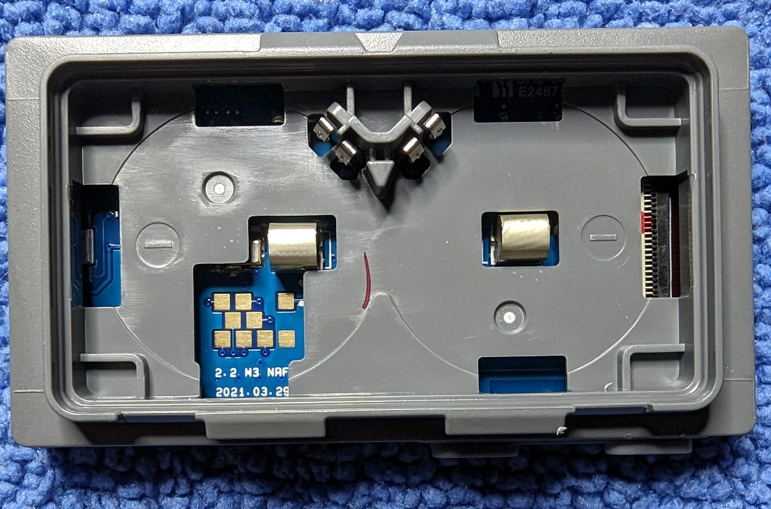
All programming pins are accessible from the rear once the batteries are removed.

Batteries are held in with moulded plastic clips.
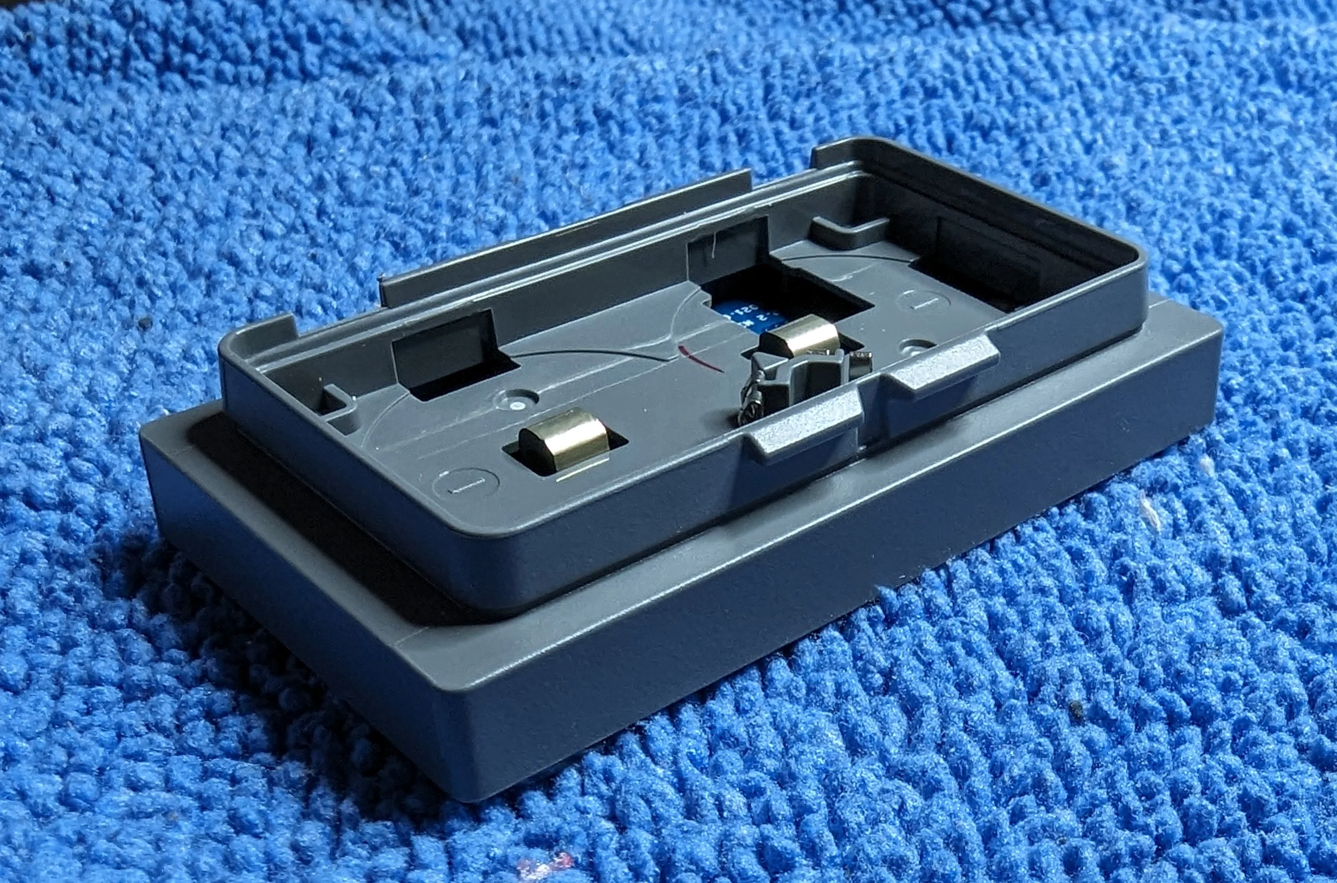
Side profile of the ESL.
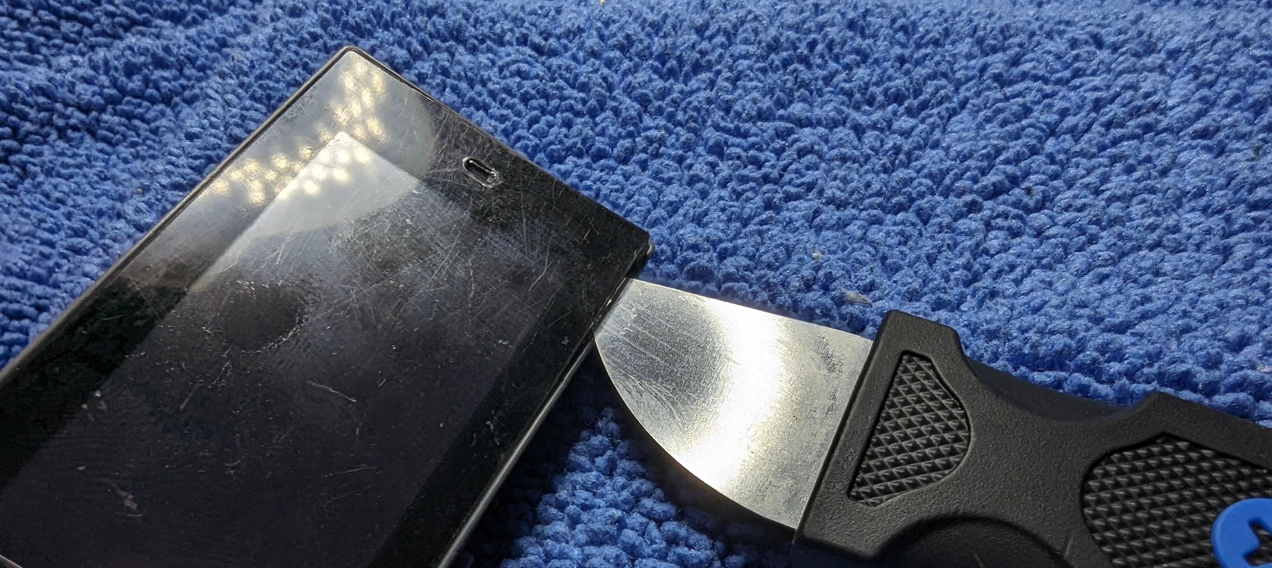
The outer front panel is glued in place. Careful prying was enough to remove it.
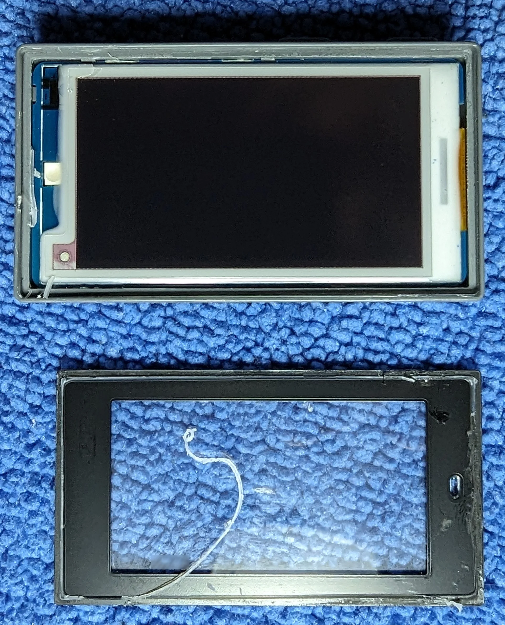
Unfortunately, there's more glue holding the eInk panel to the PCB and the whole PCB assembly in the case.
DO NOT DO THIS.
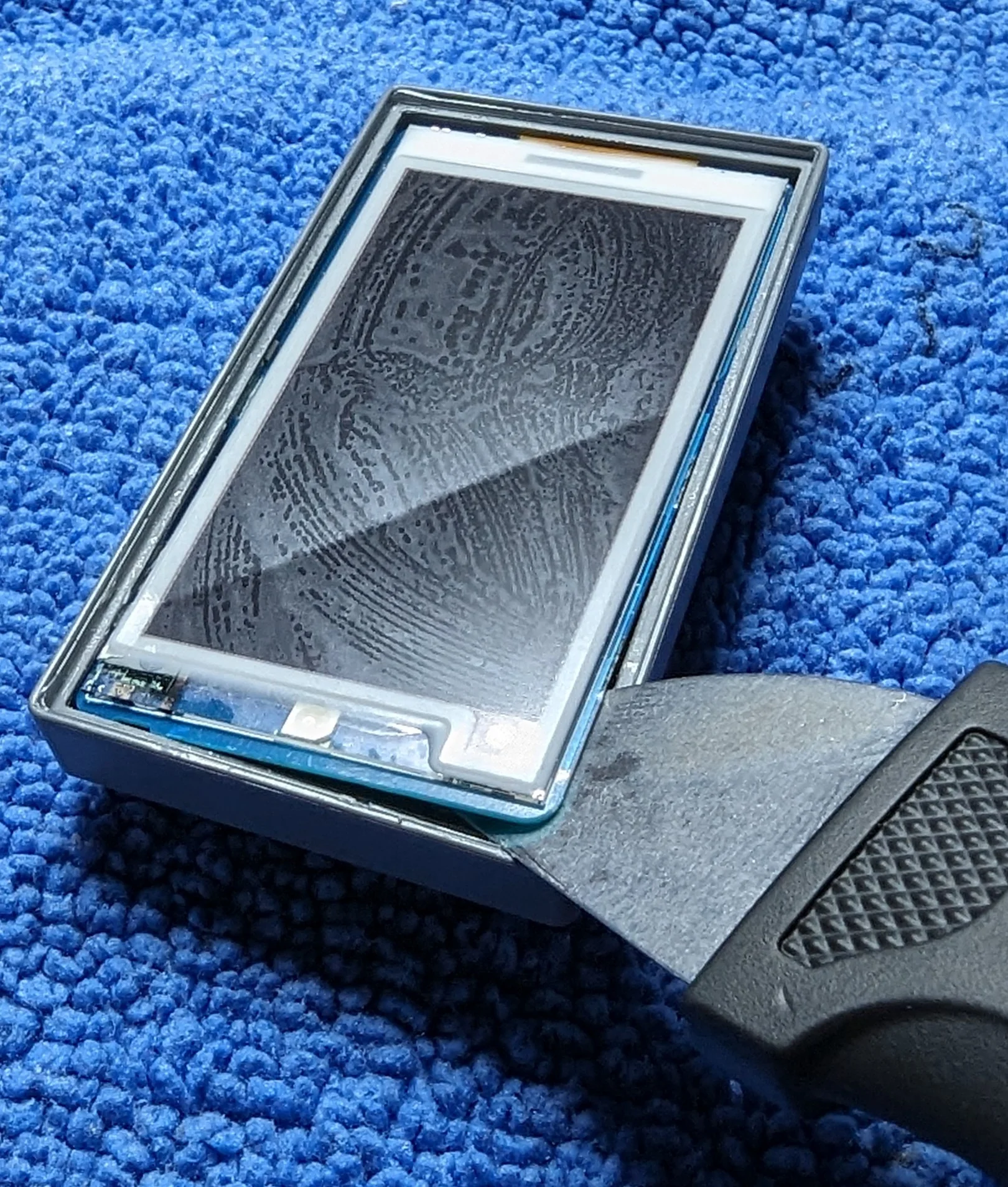
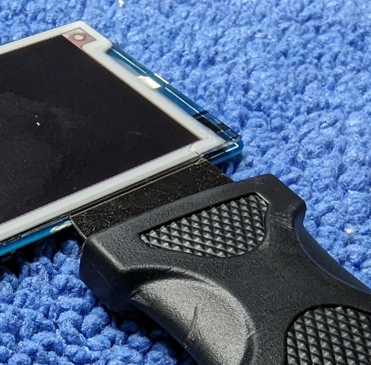
The PCB can be pried out of the case but doing so will likely damage the eInk panel unless you apply pressure equally from multiple corners.
The glass on the eInk panel is very thin and far less flexible than the PCB. Note the crack…
The residue is not there by default. Since I had already ruined the panel, I was testing the effect of different solvents on the panel hoping to find one that would dissolve the glue without damaging the panel.
The eInk panel is attached to the PCB with a thin layer of glue. The same tool/technique used to remove the front panel can be used to remove the eInk panel.
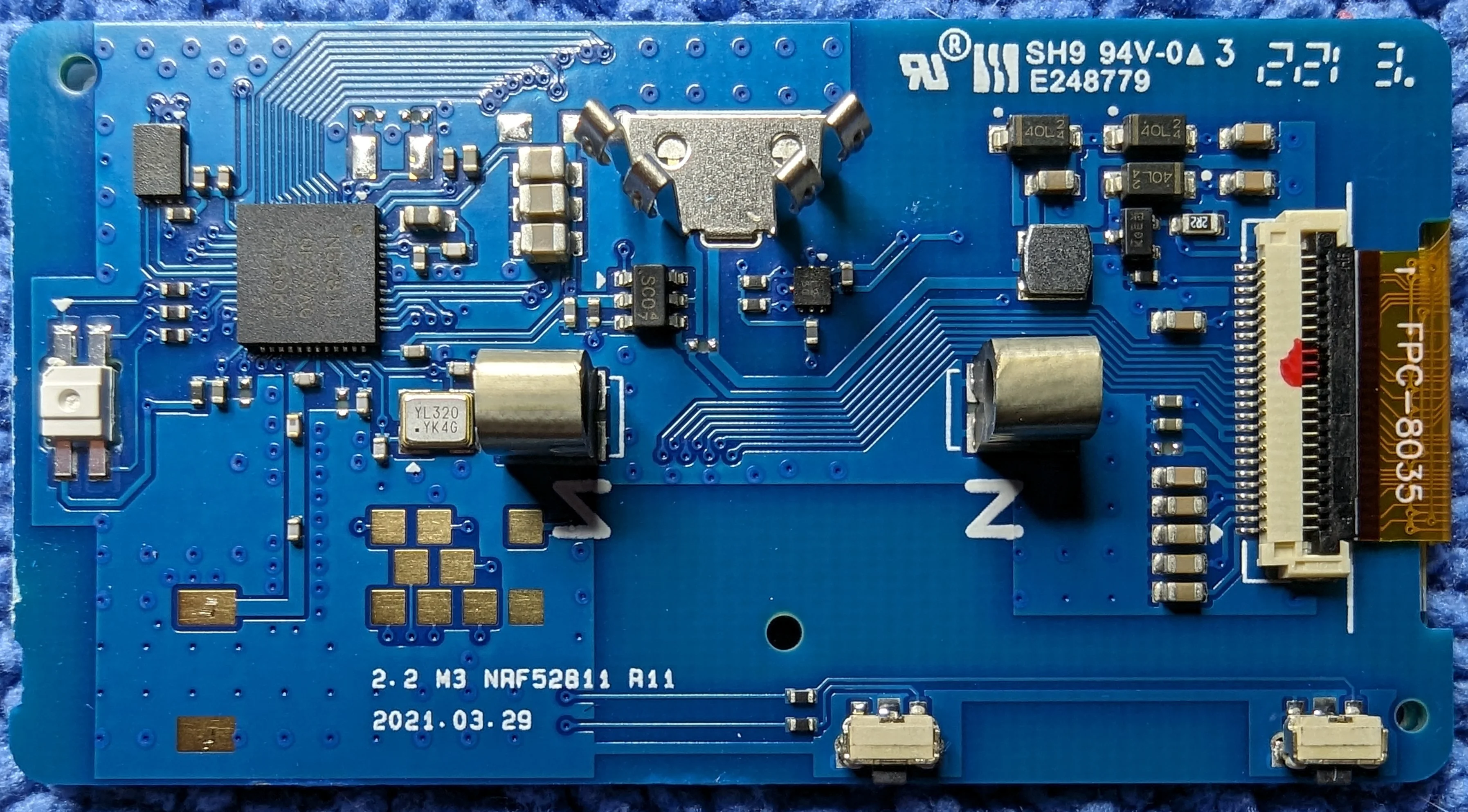
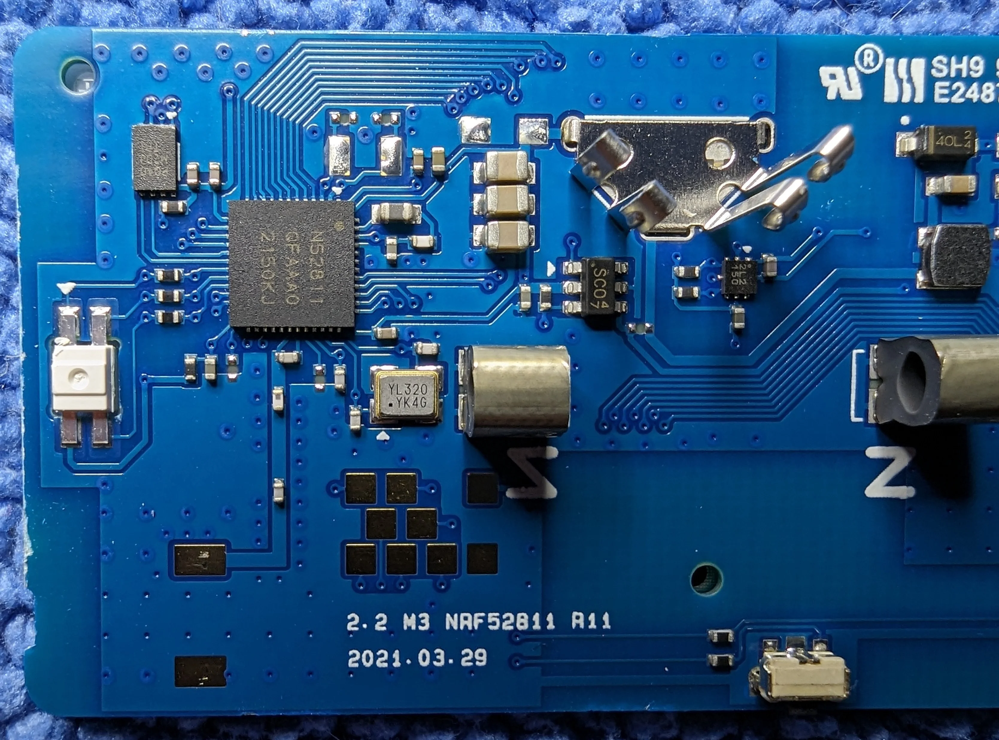
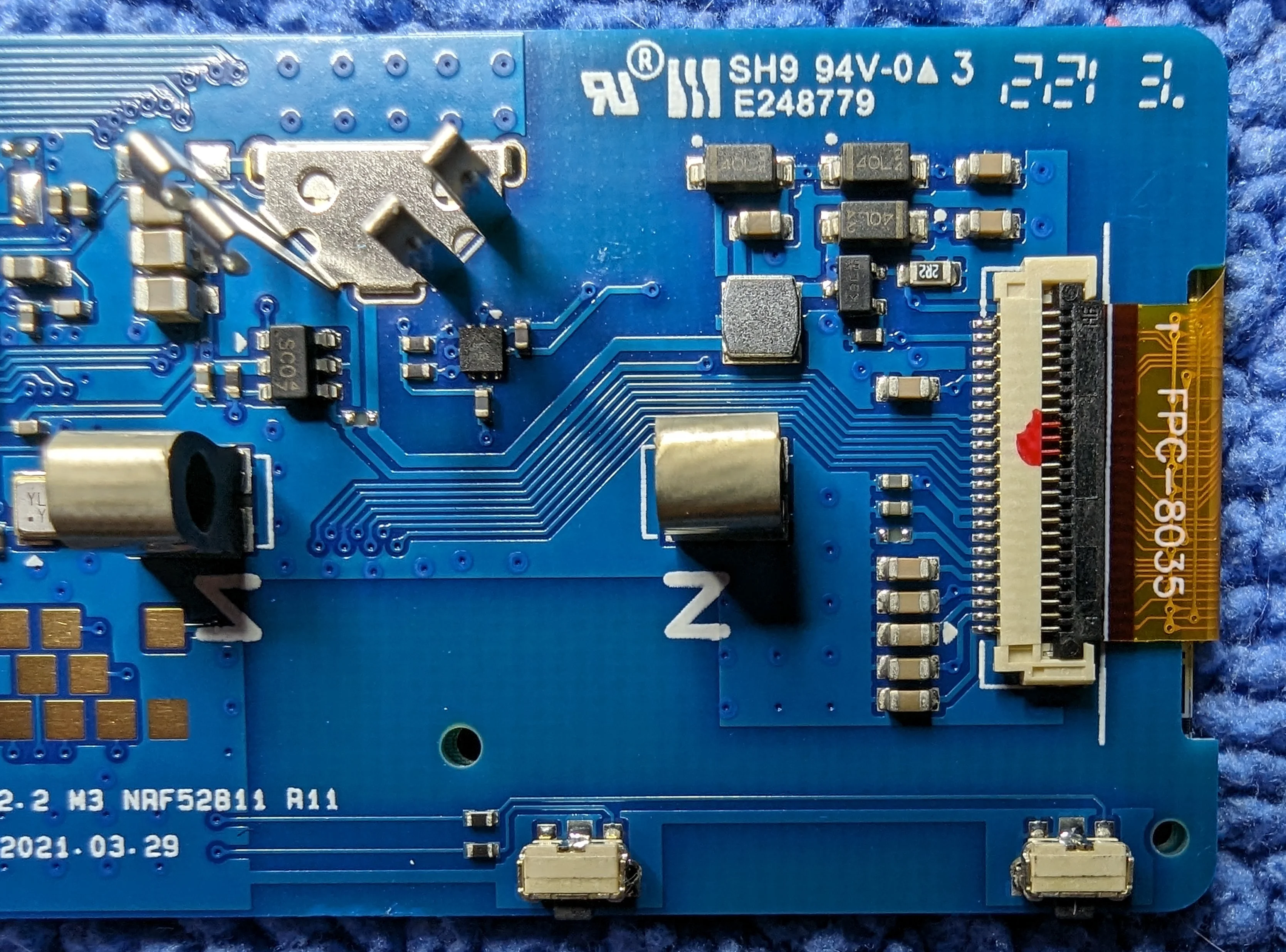
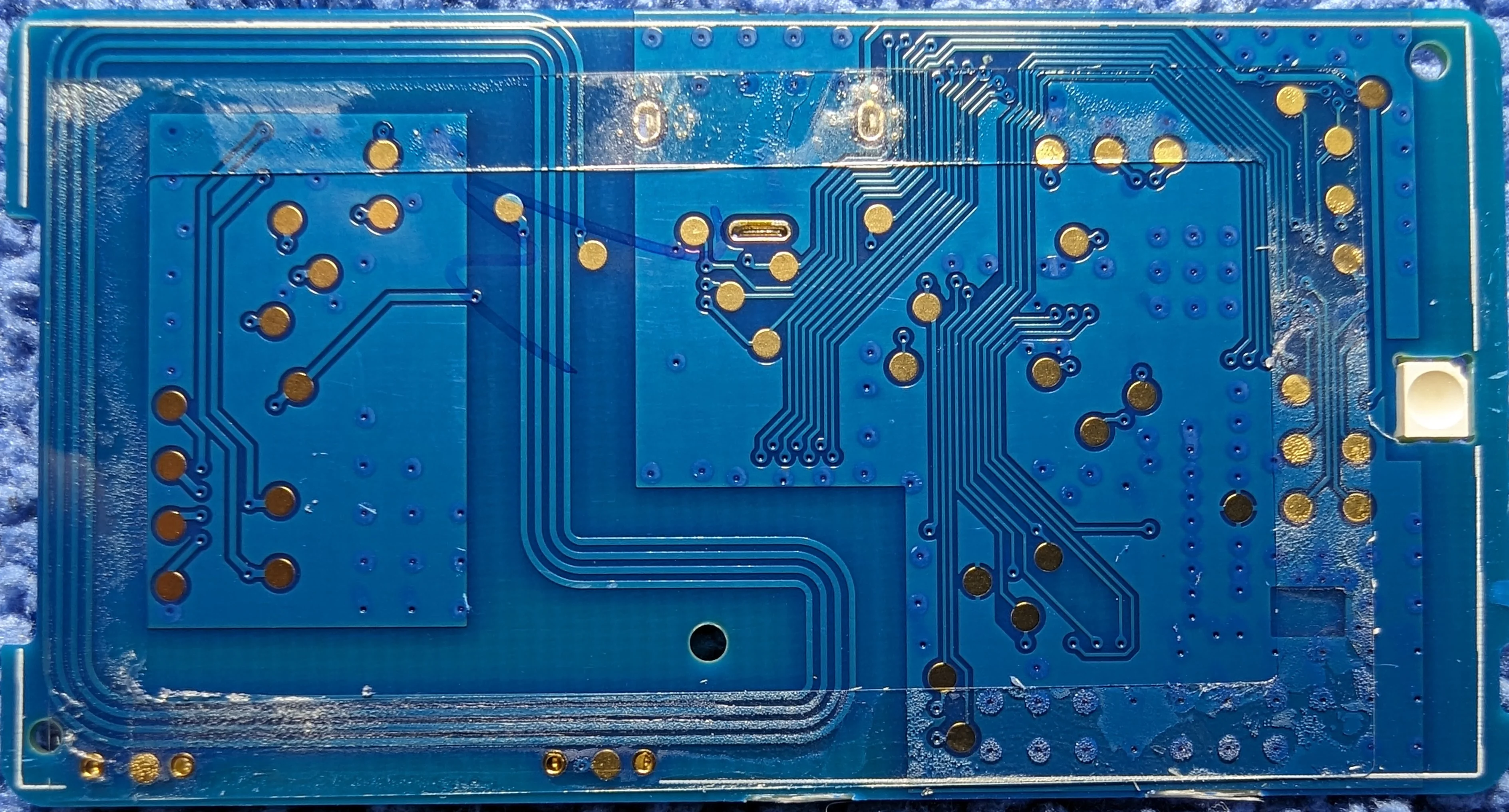
PCB as seen from the rear of the ESL. A close up look at the micro and related pcb traces. Close up look at the second half of the PCB. Closeup of the side of the PCB normally covered by the eInk panel. Note the thin layer of glue around the edge of the PCB used to hold the eInk panel in place.