Shelly Pro 4PM teardown
Yet another teardown post!
Curiosity got the better of me while putting together a BOM for a project and I decided to add one of the new Shelly devices to my order to bump the total over the threshold for a nice discount.
I have not seen a ton of discussion about what’s inside of a any of the new Shelly Pro devices. These ’next generation’ devices appear to all use a common and more uniform API which, apparently, is too demanding of the ESP8266 based hardware so it won’t be backported.
A cursory google only reveals some light technical details from a teardown post on a german site. All of the pictures attached ot that post require a login 🙁.
So here is my teardown. No login required!
What
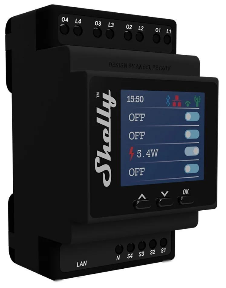
The Shelly Pro 4 PM is a rather compact DIN mounted relay/power monitoring module with some connectivity. The 4 is for the number of channels that can be independently switches and monitored.
As for connectivity, the official product page sums it up nicely:
Professional 4 channels relay with Wi-Fi, LAN, and Bluetooth connection, suitable for home and facility automation with remote control and precise power management. DIN rail mountable inside a breaker box. Enhanced safety features and compatible with most used home automation platforms.
Teardown
This Shelly 4PM feels like a step backwards in terms of build quality. The prior generation of devices were very dense little pucks and this feels pretty hollow; the plastic DIN case creaks and squeaks.
The internal layout isn’t my favorite and it made both disassembly and reassembly a bit tenuous at a few points. The layout may be inevitable, though, as DIN case is more or less a standard shape and size. Layouts are almost always a bit weird when the electronics have to be designed to fit the case rather than the other way around.
Other than the layout quirks, the Shelly team continues to go with what they know: the espressif line of chips. This time the ESP826x series is out and the much more capable ESP32 series is in… which allows for both the color LCD and the ethernet interface.
As is common with these types of devices, the ESP runs the show… but it has a few deputies: dedicated power monitoring ICs and an ethernet PHY.
And with that, let’s get into it:
The main body of the shelly is clipped to the rear ‘plate’ which houses the DIN rail attachment mechanism. You can see the clips on the very top and bottom along the left edge:
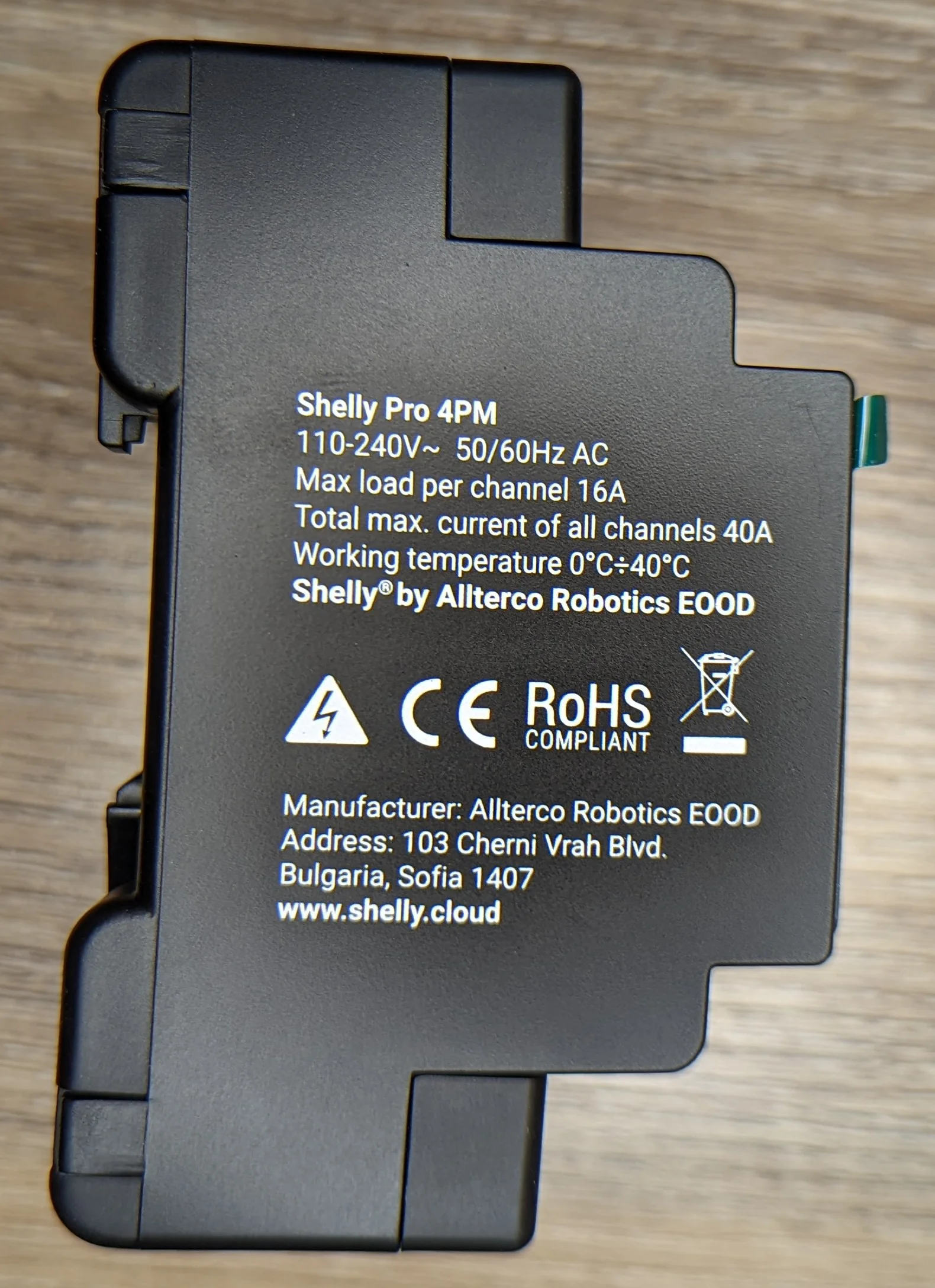
40A at 240V is a _lot_ of power to fit into a fairly compact device!
Viewed from the rear, the clips are easier to see in the four corners:
The rear plate lifts off to reveal the largest PCB. There are 4 copies of the same circuit. Very nice to see big traces with extra solder and some beefy current shunts!
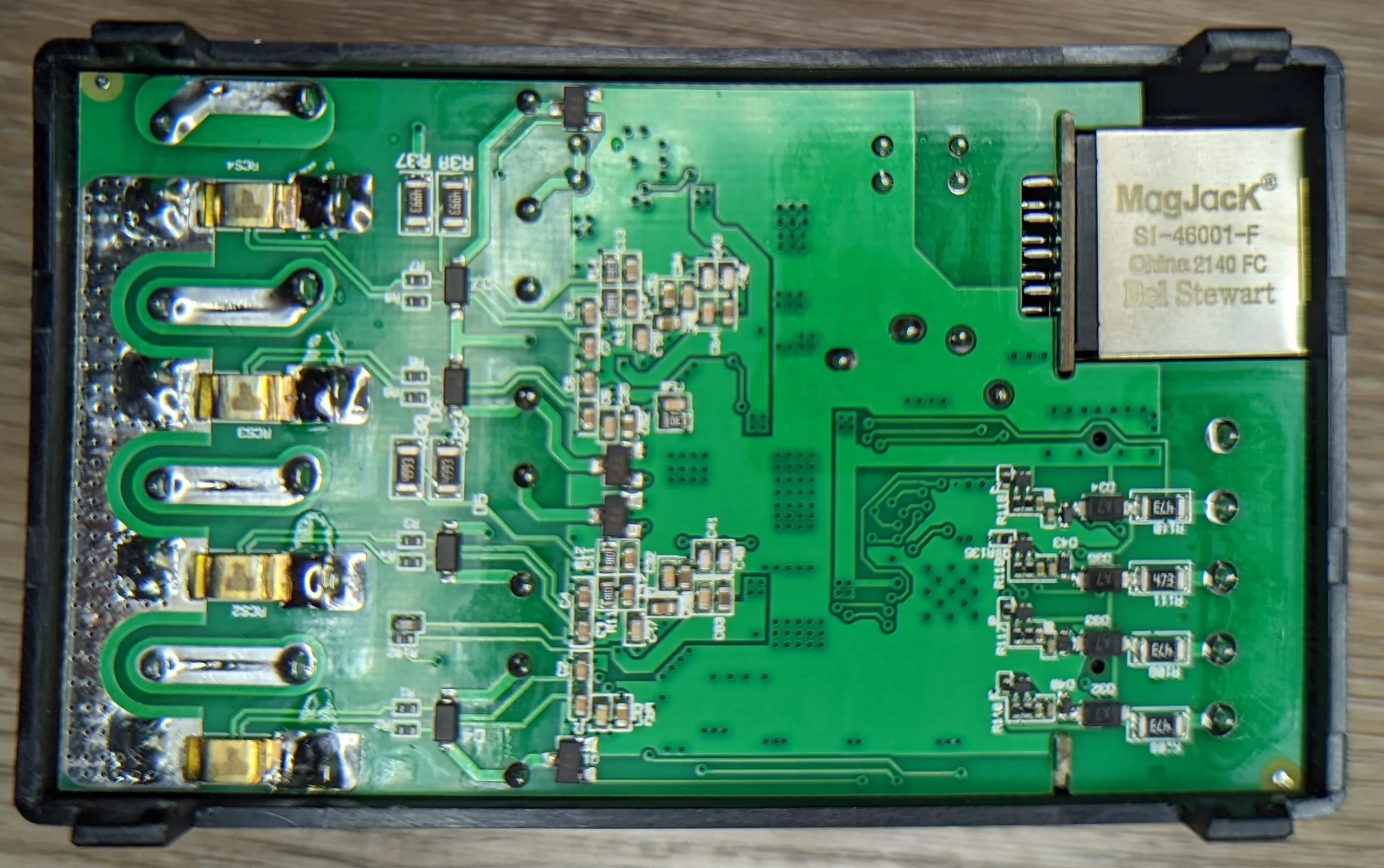
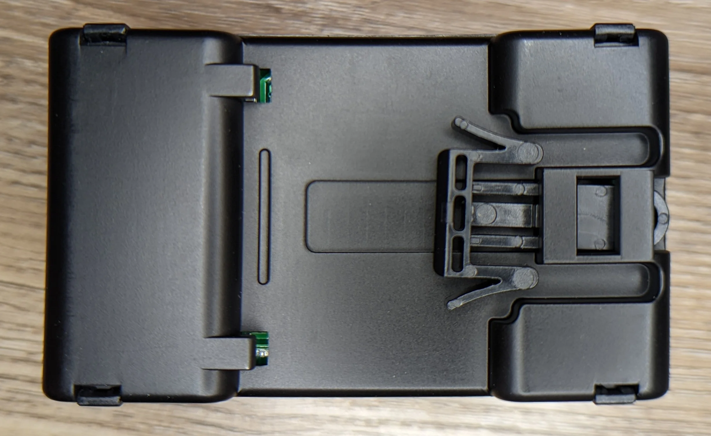
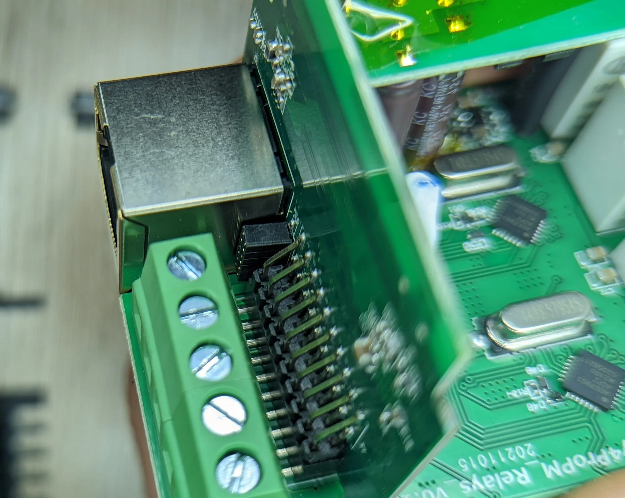
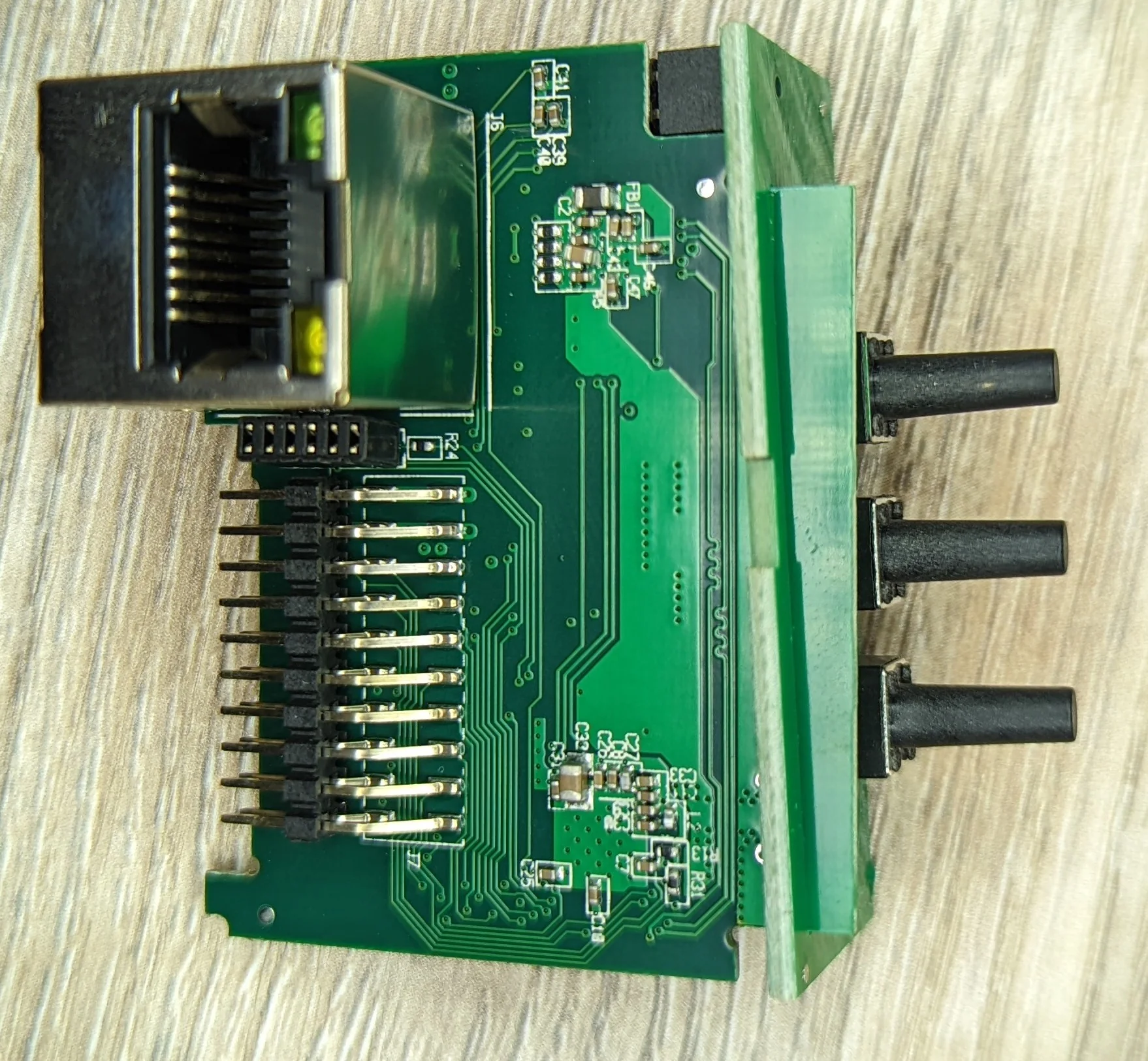
Just behind the ‘input trigger’ terminals on the main PCB is a 2x10 @ 2.54mm pitch female header. Into which slides the ‘smarts’ PCB which hosts the main ESP32 MCU as well as the ethernet jack.
On this smaller PCB and next to the ethernet jack is a very small 1x6 @ 1mm pitch female header block. It is cleverly hidden next to the jack but could probably be accessed with the case on if you’re careful.
If I had to guess, this is a debug/programming header for at least the main MCU.
It’s not pictured until later, but there is a 2x2 @ 2.54mm pitch male header block on the other side of the smarts PCB. This is where a small daughterboard containing only the 3 buttons connects.
How much do you want to bet that the pins on the debug header are the usual +3.3, GND, IO0, RX, TX for ESP flashing?
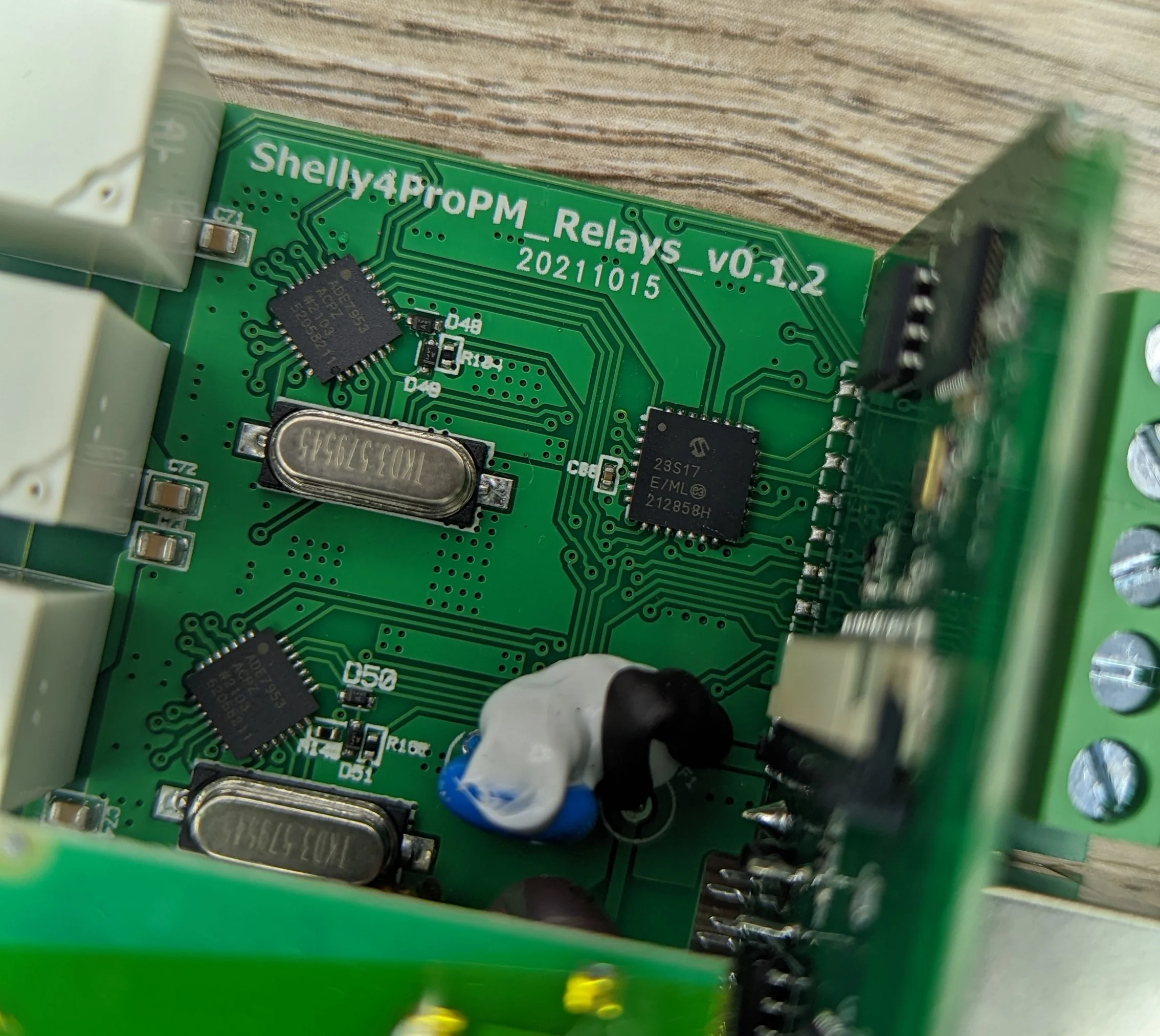
On the main PCB, behind the ‘smarts’ PCB is a set of two ICs marked with ADE7953ACPZ. As expected, these are the energy management / monitoring ICs.
Why two crystals, though?
The IC marked MCP23S17 is a simple SPI based IO expander… almost certainly used to drive the relays and possibly command the power management ICs.
On the rear of the ‘smarts’ PCB is the star of the show: ESP32-D0WDQ6.
In addition to the passives and the flat flex socket for the LCD, we have:
- cFeon QH64-104HIP 64 Megabit flash chip
- SMSC8720A: 10/100 Megabit ethernet PHY
There is also another daughterboard covered in kapton tape. This is soldered to the main PCB and just has a few electrolytic caps. I guess this arrangement was easier than trying to clear some room on the back of the main PCB so the heavy current traces could be kept simple 🤔?
In the top right corner you can see the 4 pin header where the button daughter board attaches… just next to the ethernet phy.
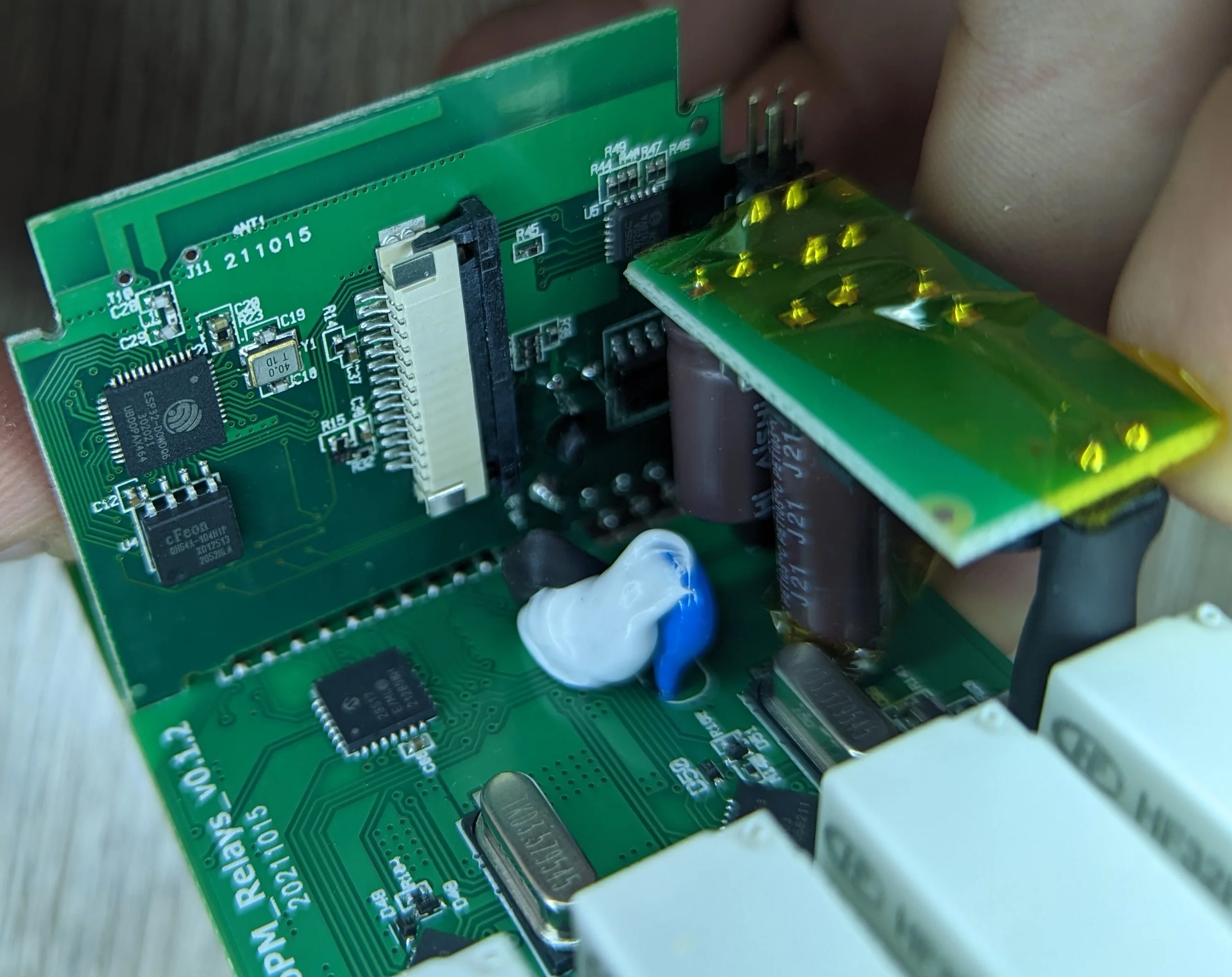
From this angle, still in the top right corner, you can see the button daughter board attached to the 4 pin header.
Just a few very tiny passives!
Electrically, nothing unusual or bizarre. Layout was a bit ‘inventive’ but the unusual but standard shape of the case probably drove at least some of the decision to have 4 different PCBs that all have to be tediously connected by hand during manufacture!
Thats all for this one!
PCB/IC Markings
AKA SEO optimization 😉
ADE7953ACPZ: Power monitoringMCP23S17: IO expansionESP32-D0WDQ6: main CPUEN25QH64: 8 MB flash chipPrimary PCB is marked:
Shelly4ProPM_Relays_v0.1.2Daughter boards not really marked with anything other than the usual component IDs and the date code of
211015