Altinex TE460-137 Teardown
Altinex TE460-137 Teardown
It is surprisingly hard to find a device that can dump details about the various protocols and negotiated standards for a HDMI connection. For how ubiquitous HDMI is, you’d think that there would be a lot of devices that can do this. There are LOADS of devices that can snoop USB and Ethernet, but HDMI is a bit of a different beast, apparently.
After a bit of searching, I found the Altinex TE460-137 could do exactly what I wanted.
(/enhanced-homeassistantswitchplate/) project.
Like the HDMI CEC dongle this device is a bit specialized and so there’s not a lot of readily available information about it online. I was curious about what’s inside and how it works, so I decided to take a look.
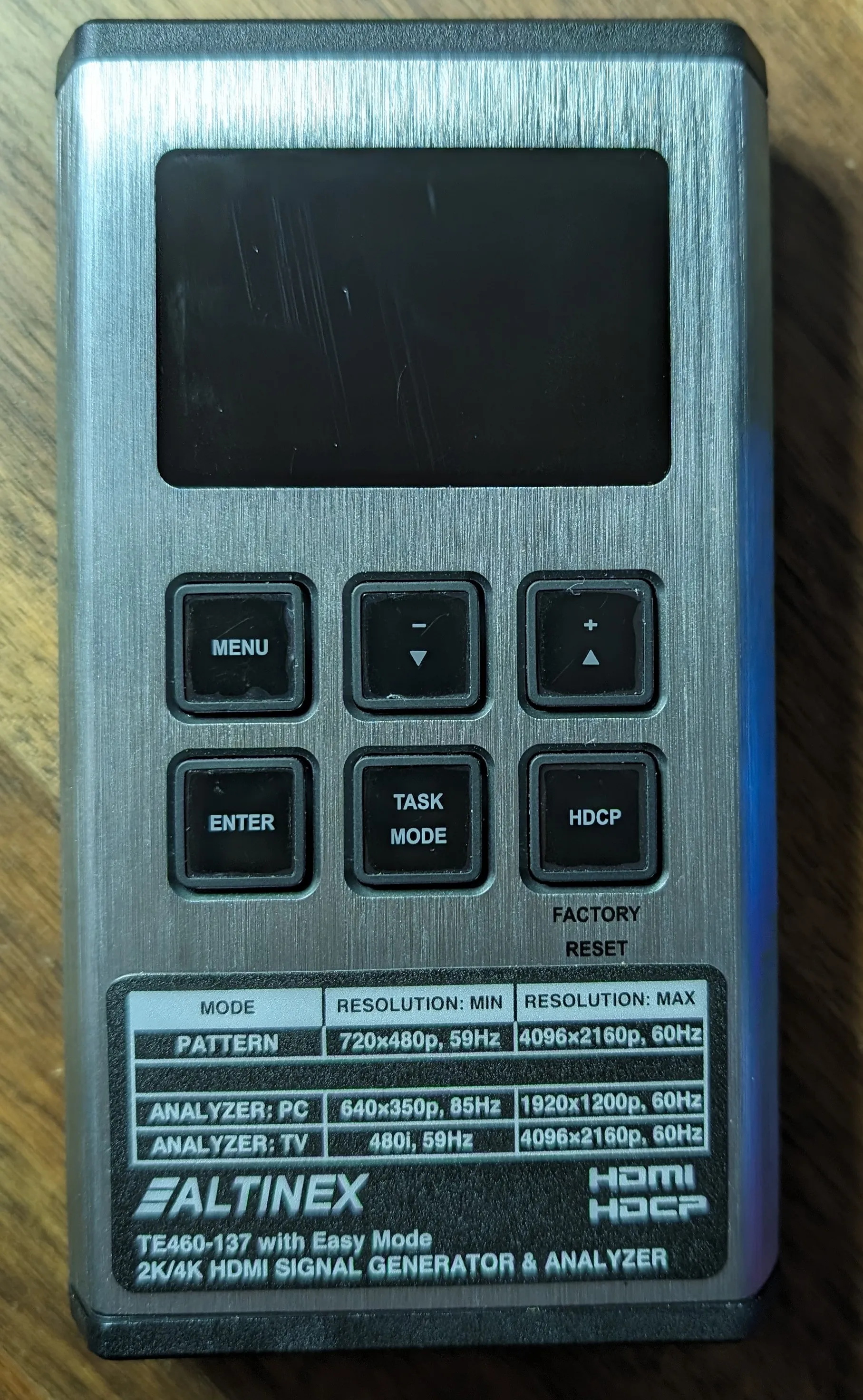
Front of the device.
Magnuson-Moss Warranty Act
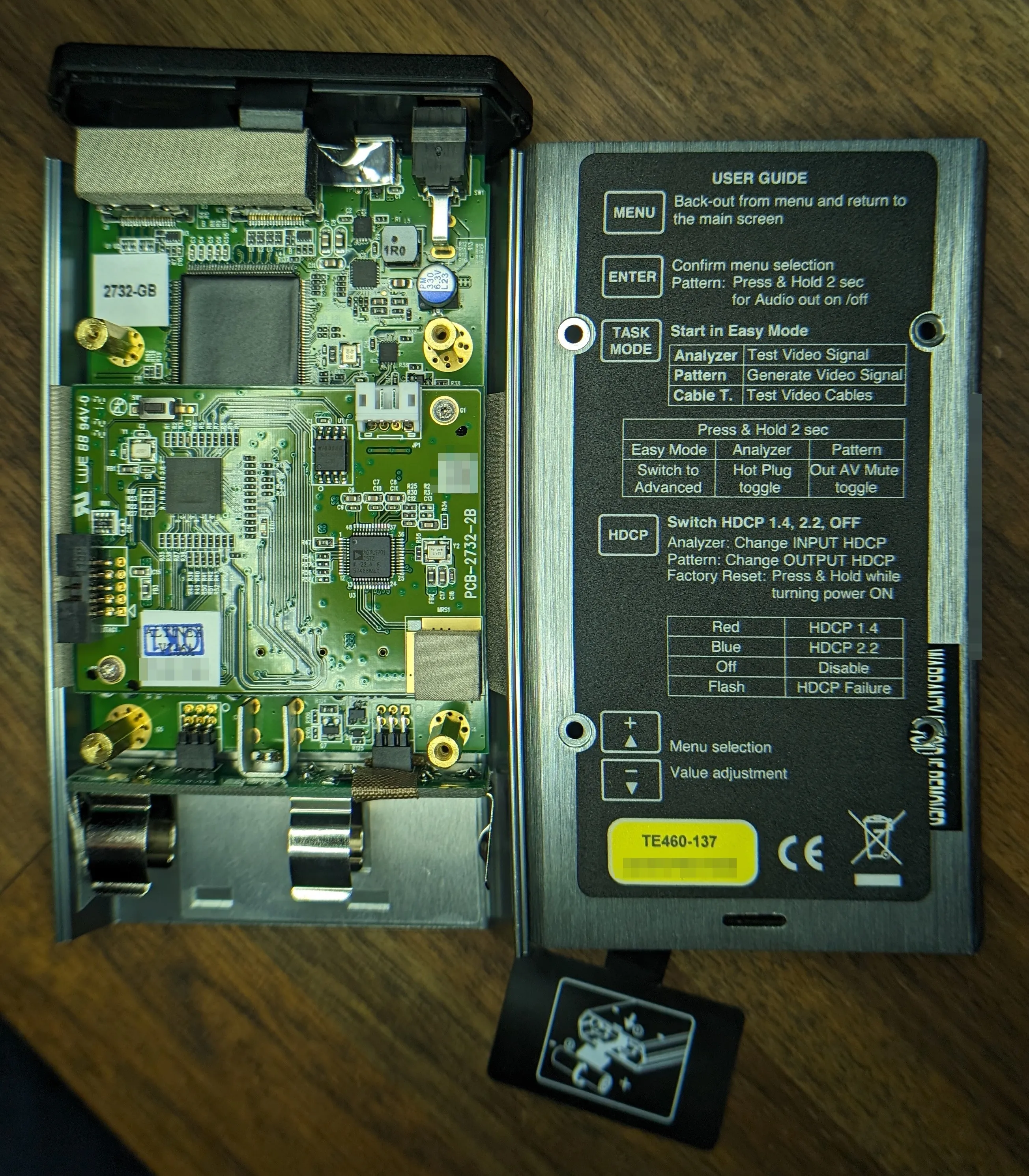
The case split open.
Notice that pierced Warranty void if removed sticker over the bottom right screw?
Yeah, that’s illegal.
Naturally, companies don’t want you to know that the sticker is unenforceable.
Consider this a small PSA: if you see a sticker like this, you can safely ignore it. The company cannot void your warranty for removing it but they absolutely can make your life difficult if you do. If you get pushback, direct them to the FTC’s official statement on the matter.
Anyways.
Quick peek Inside
After removing the four screws, the case splits open easily enough. The construction is a bit more elaborate than expected; there’s a main PCB, a control PCB, and a battery interface PCB.
I was in a hurry so the photos are “as-is” and not my best work. I’ve noted down the markings on the chips and other components for future reference.
Internals feature three PCBs.
If the battery ever does leak, the entire PCB assembly can be removed and replaced. It also shouldn’t be that difficult to just modify the battery interface PCB to use a different battery. The thermistor is a nice touch!
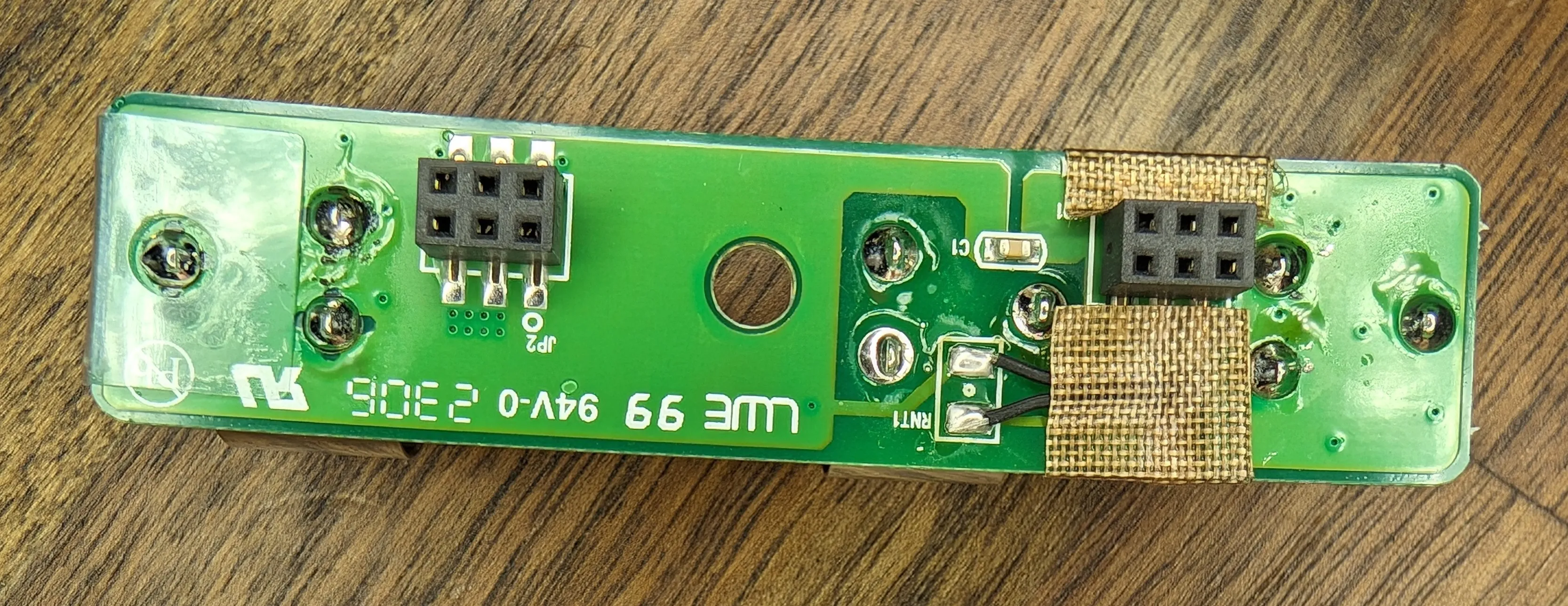
Rear of the battery interface PCB.
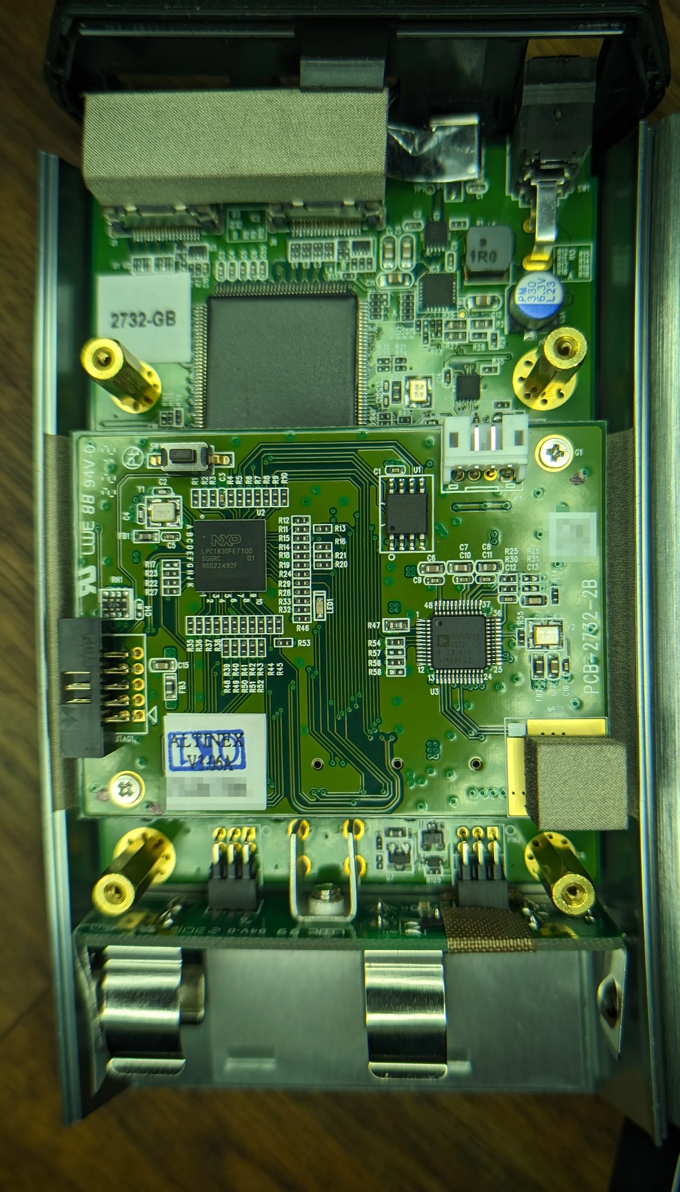
Taking a quick look at the control PCB, we can see a few big ICs… The populated JTAG header is an interesting find.
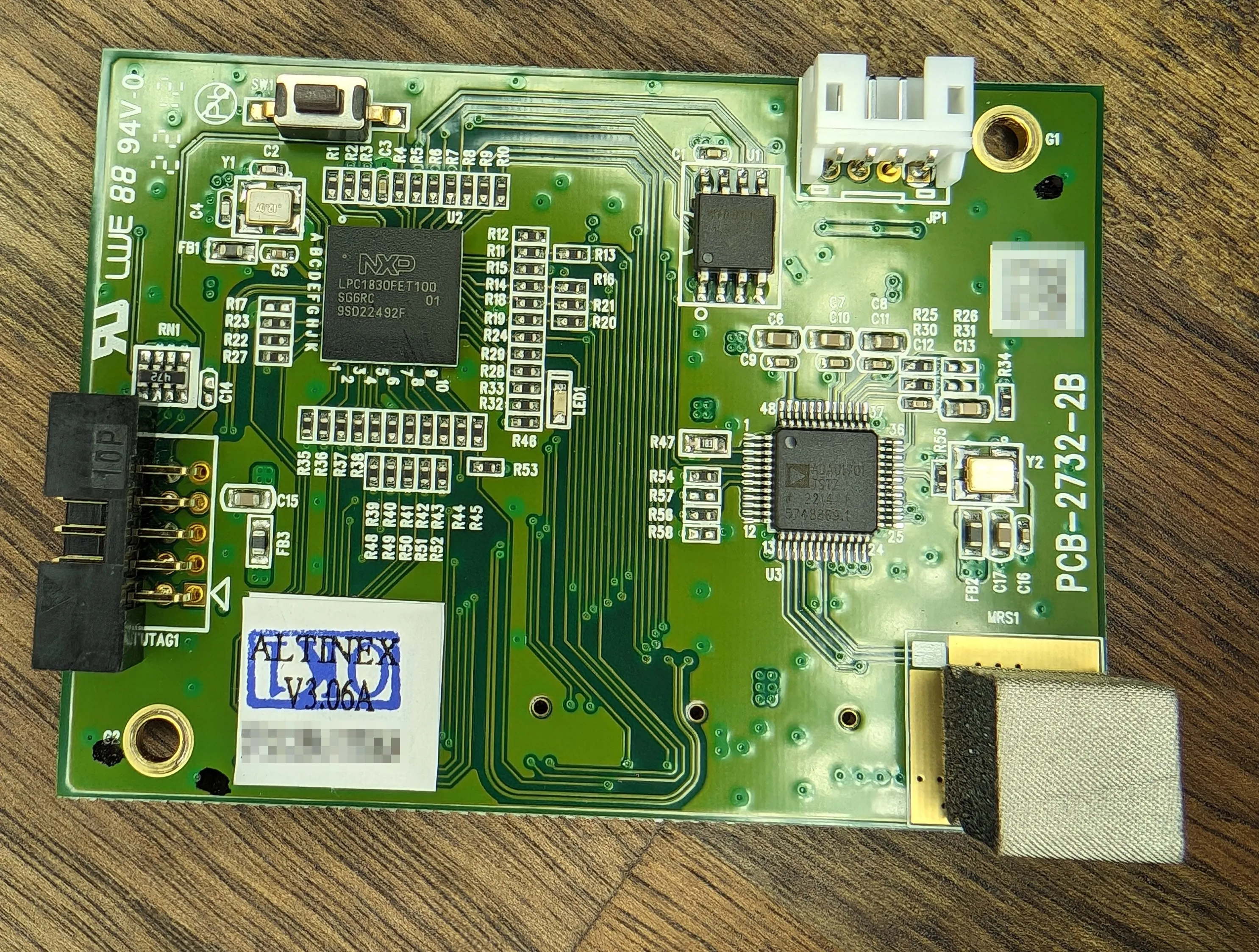
Top of the control PCB.
There’s not much on the rear of the control PCB:
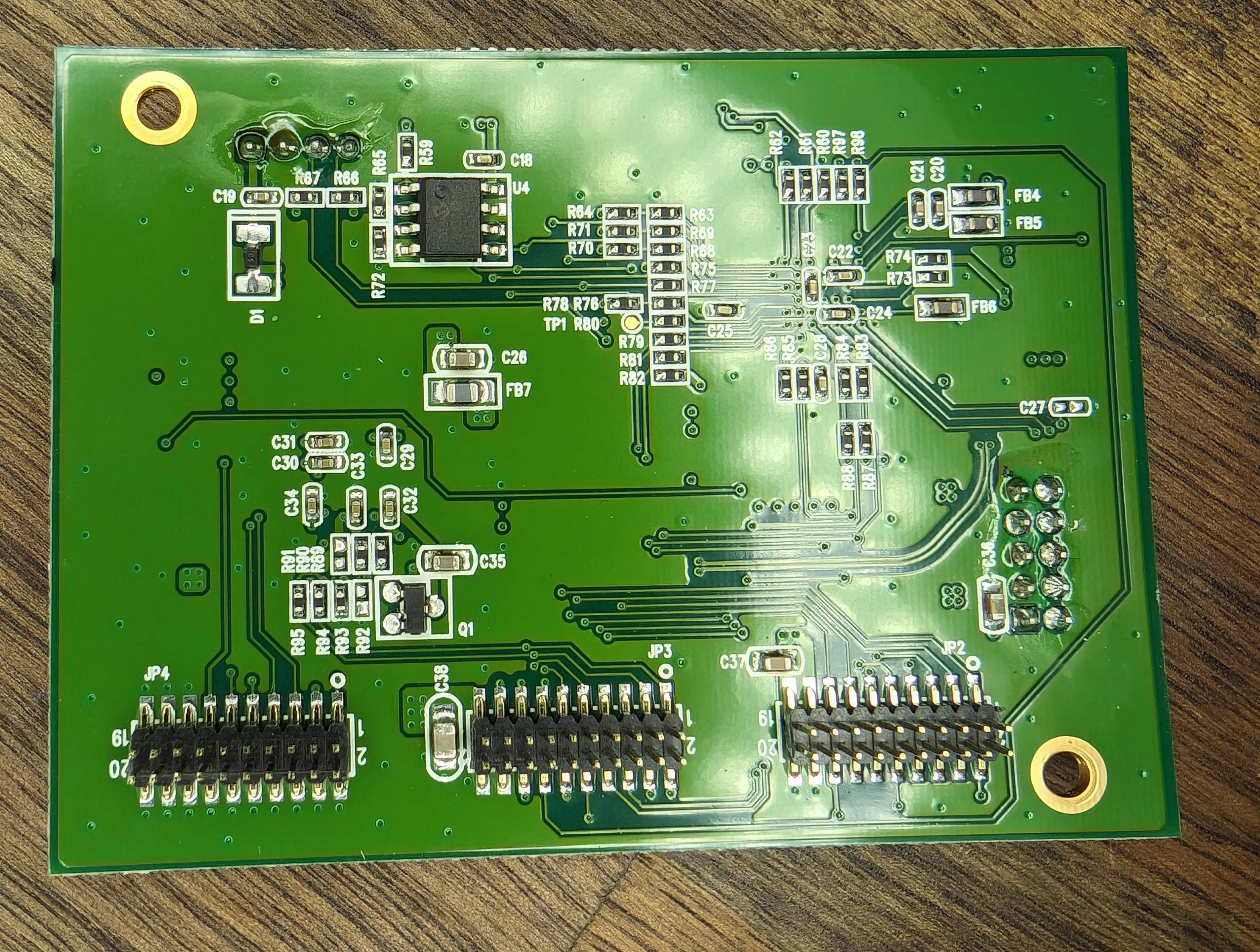
Bottom of the control PCB.
Nor is there much on the side of the PCB just behind the OLED screen / front panel. Oddly enough, each button gets two sets of contacts…
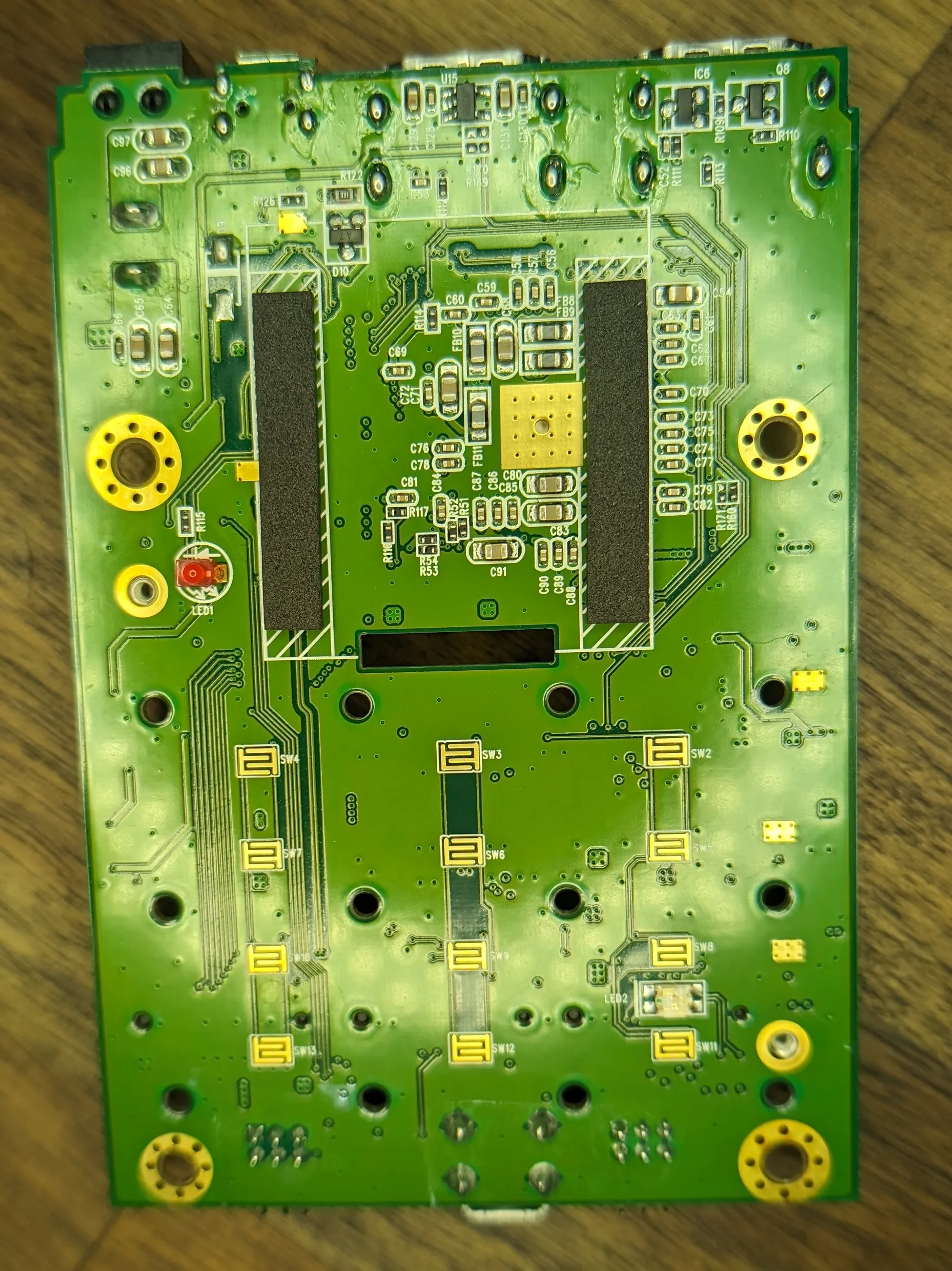
The side of the main PCB that faces the user from within.
And there’s nothing interesting on the ‘internal’ side of the front panel:
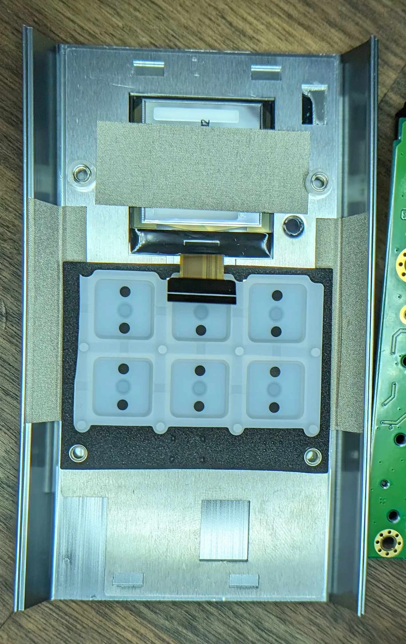
Interior of the front panel features button matrix and OLED.
Some Technical Details
If you catch the device early enough in boot, you can see the panasonic HDMI switch chip enumerating in it’s default state. Don’t ask me where the 2% overscan comes from…
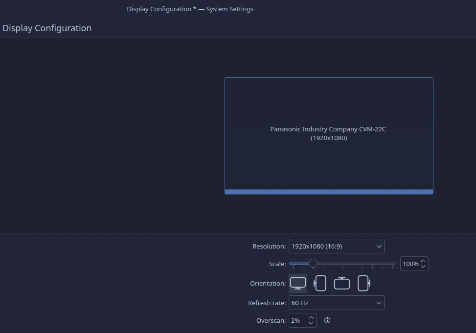
The default EDID info doesn't last long; as soon as the device is powered on, it tries to read the EDID from the connected sink and use that.
Chips and other markings
Control PCB
- The main application processor is the NXP LPC1830FET100.
- It seems like all audio is handled by the Analog Devices ADAU1701.
Oddly enough there are two flash chips here. Presumably firmware storage for the NXP and Analog Devices chips.
I didn’t bother dumping either, but Altinex does make an older version of the firmware available.
Main PCB
The big QFP144 chip on the main PCB is a Panasonic MN864788. I can’t find a data sheet, but one supplier has labeled it a “HDMI 2.0 Receiver/Switch”. Given the proximity to the two HDMI ports … this makes sense.
dmesg
For thoroughness, here’s how the device enumerates over USB when plugged in when configured in RS-232 mode:
| |
And when in FW update mode:
| |
Firmware
The device ships with FW 3.06A/R3.
Their website only have 3.04 available.