AKASO DL12 Dashcam Teardown
AKASO DL12 Dashcam Teardown
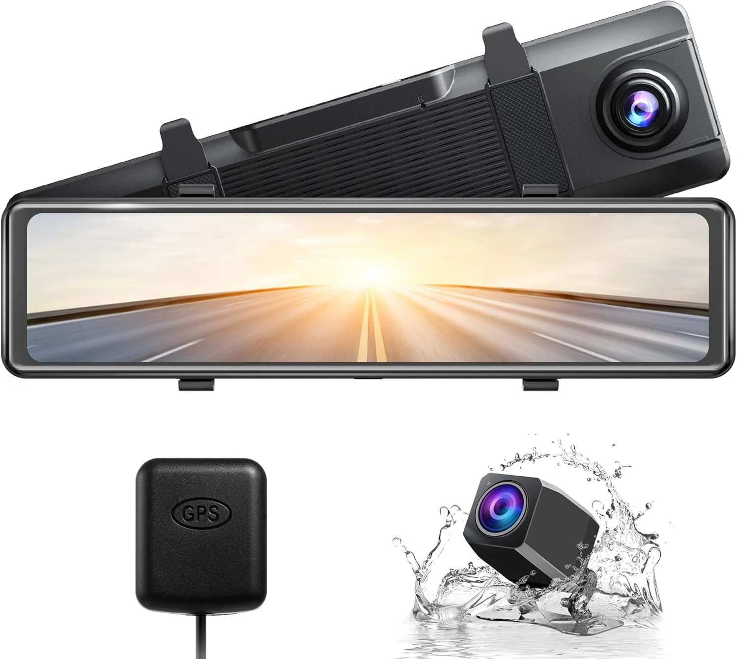
If the double yellow lines are in the middle of your rear-view mirror, you're doing it wrong.
This was my dashcam for a while until the front camera stopped working. It was a good dashcam while it lasted but there are better options now… so let’s take it apart!
Ultimately, it’s a highly integrated consumer-grade bit of electronics. Everything’s built down to a price and anything that didn’t need to be done … wasn’t. There’s not much to see and not much to say so this is a “two minute teardown” .
Teardown
There are 4 screws holding the case together. They are hidden under the rubber feet.
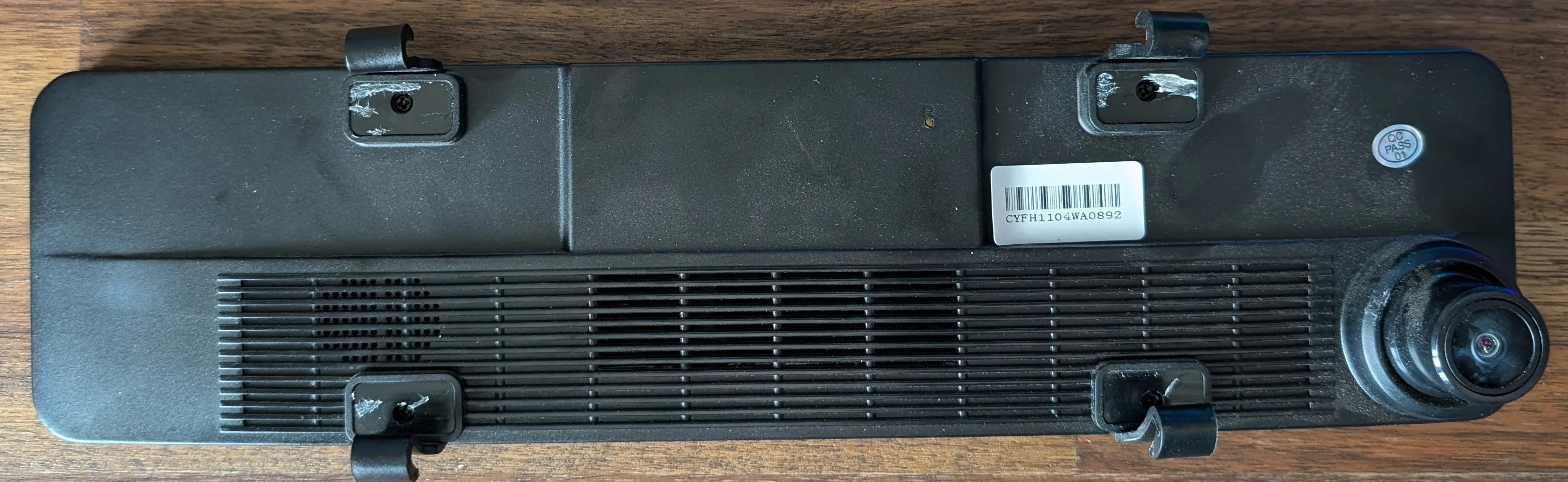
There are 4 screws holding the case together. Remove and the case comes apart easily.
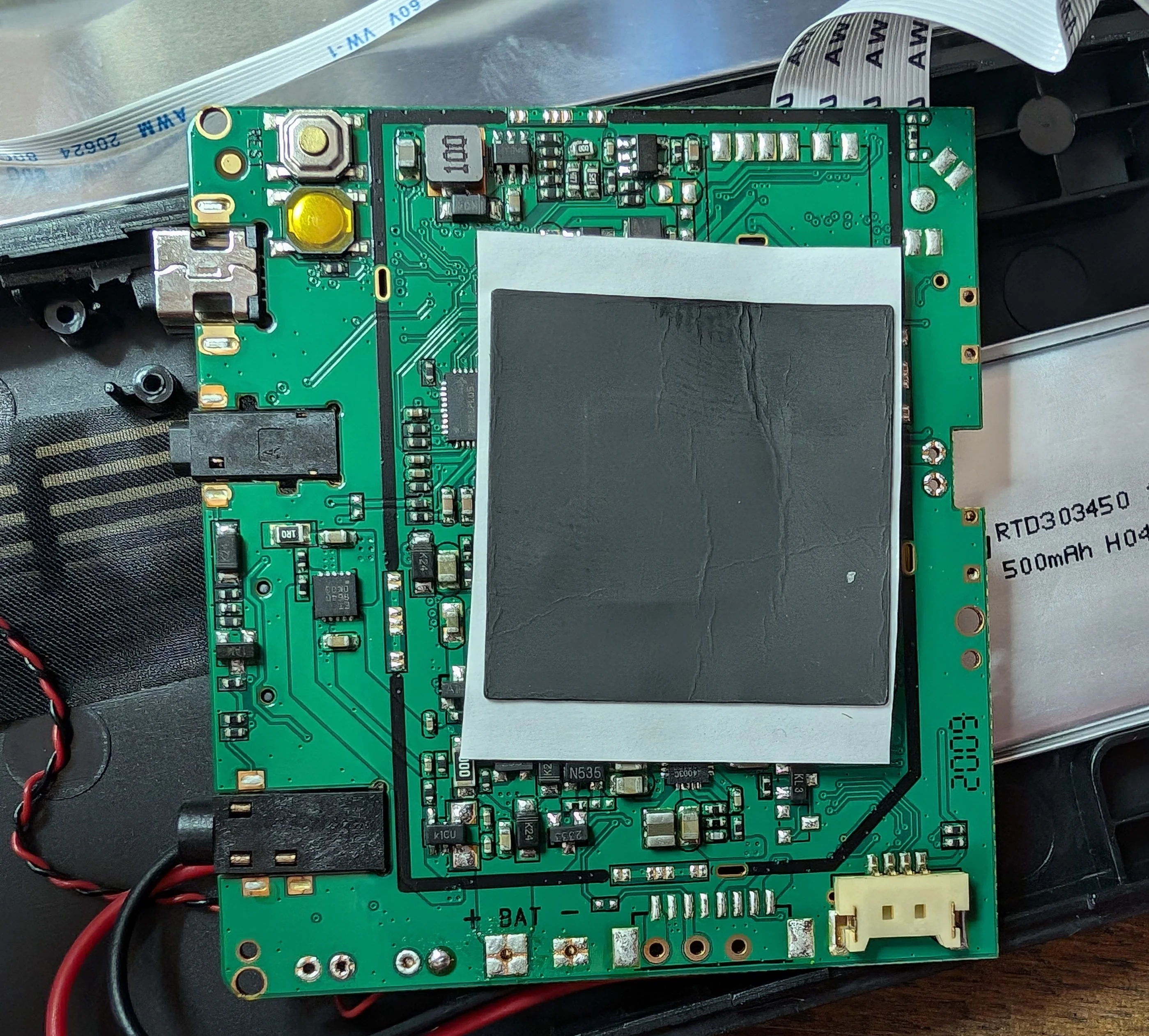
Once the screws are removed, the case comes apart easily to reveal a mostly empty shell. The LiPo battery is an interesting choice given the heat that can build up in a car. As far as I know, this is only needed for the few seconds after power loss so the camera can save the current recording and shut down cleanly.
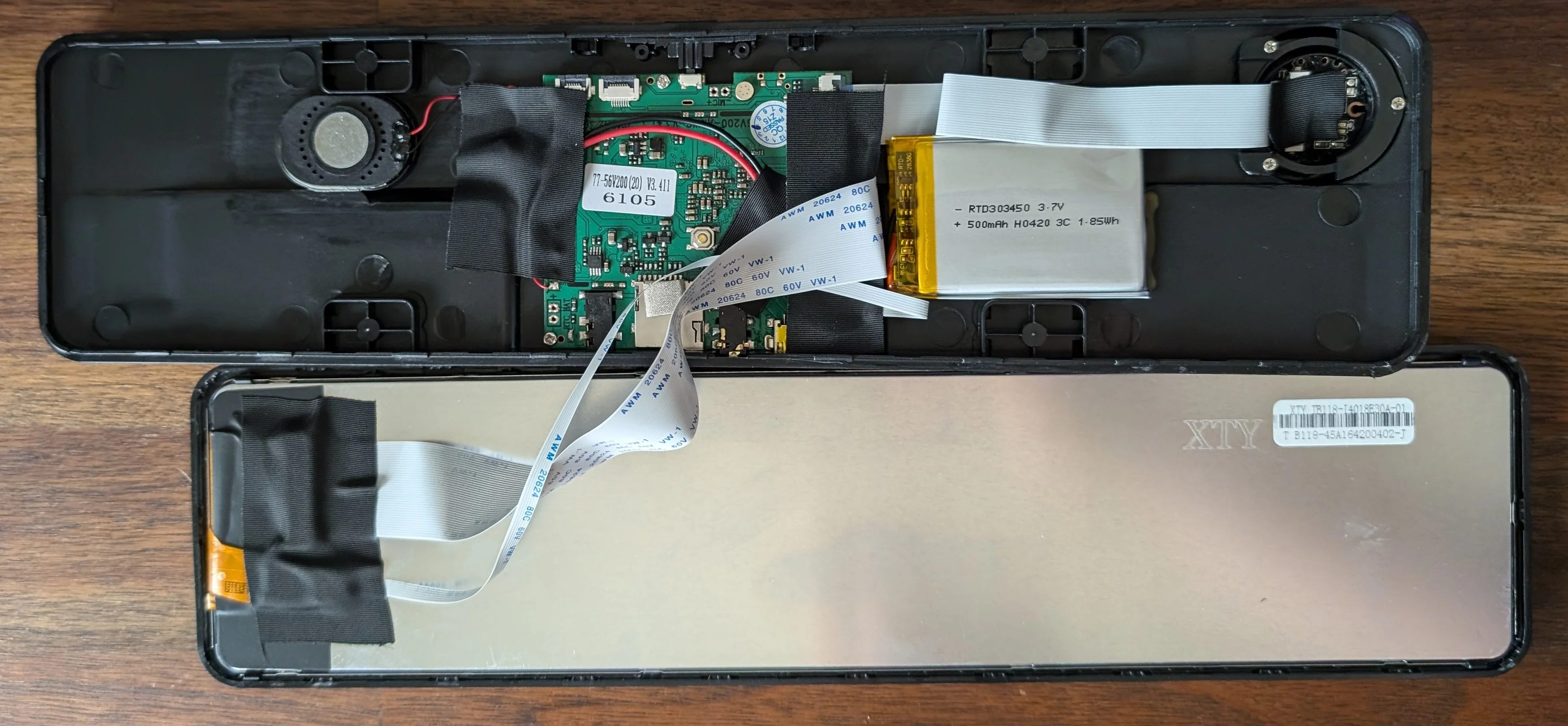
Lift the screen side away to reveal the paltry internals
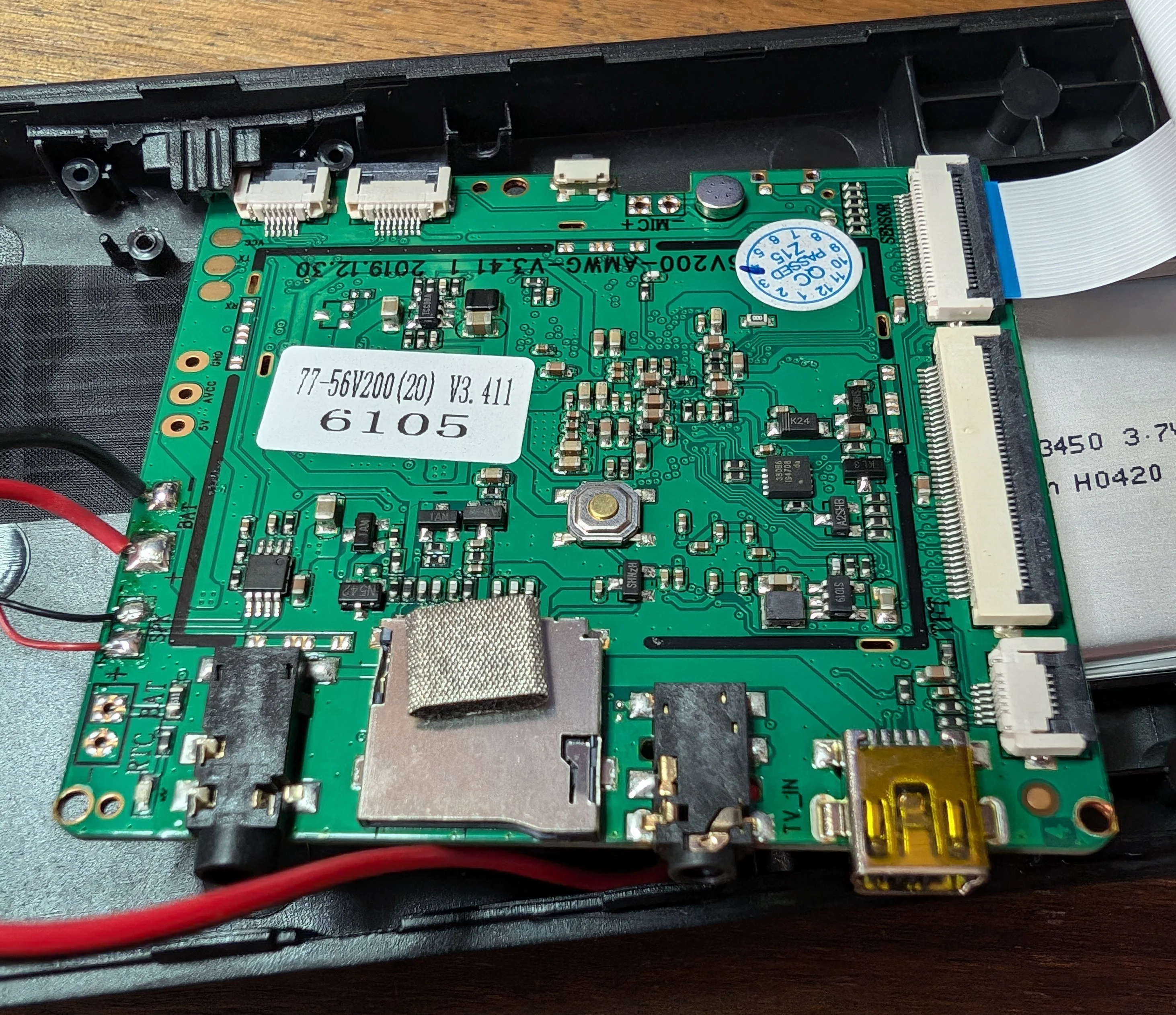
Close up of the rear of the main PCB shows a few test points and populated but unused connectors.
I love the TV_IN silkscreen for the rear camera connector. Almost makes me wonder if this was a re-purposed schematic from a different product.
Why there’s a dedicated RTC_BAT connector and not sipper power from the main battery is a mystery to me.
The unit does have a GPS module so there’s really no need for an RTC battery… just use the GPS time!
Close up of the 'screen' side of the main PCB. Not much to see here.
The ‘forward facing’ side of the PCB has a few more populated/un-used connectors and a heat-spreader over the main CPU. The two push buttons in the top left are not accessible from the outside of the case so there’s probably something interesting that happens when they’re pressed.
The 'rear' of the main PCB has a few unpopulated footprints and a flimsy heat-spreader.
Removing it reveals a HiSilicon Hi3556 SoC, EEPROM and what is probably the image processor for the rear camera. The large unpopulated footprint in the top right looks like it’s meant for a radio module. Not sure if it’s for a wireless link to the rear camera or for something like a TPMS sensor or possibly WiFi for a phone app.
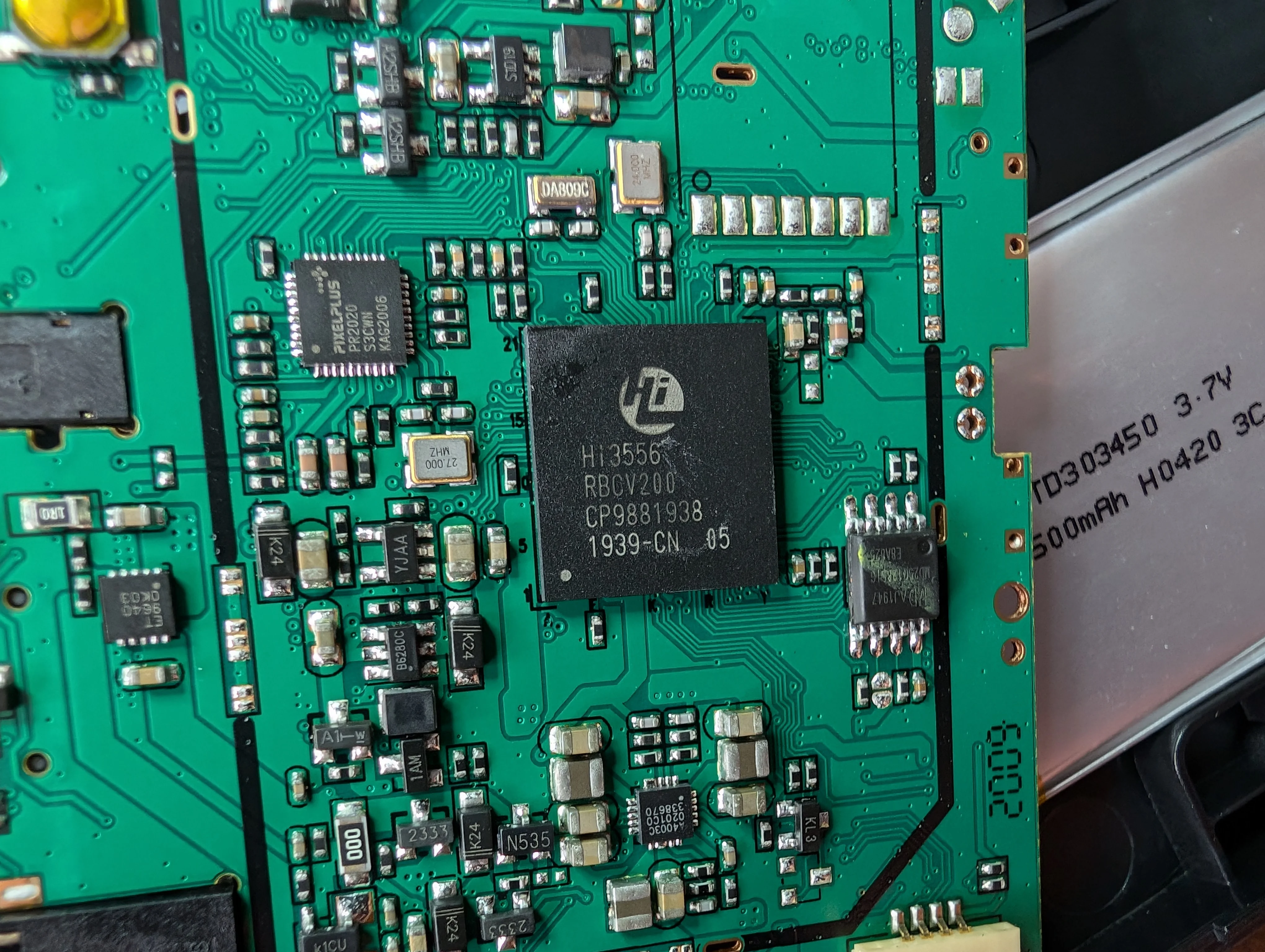
Close up of the most interesting part of the main PCB.
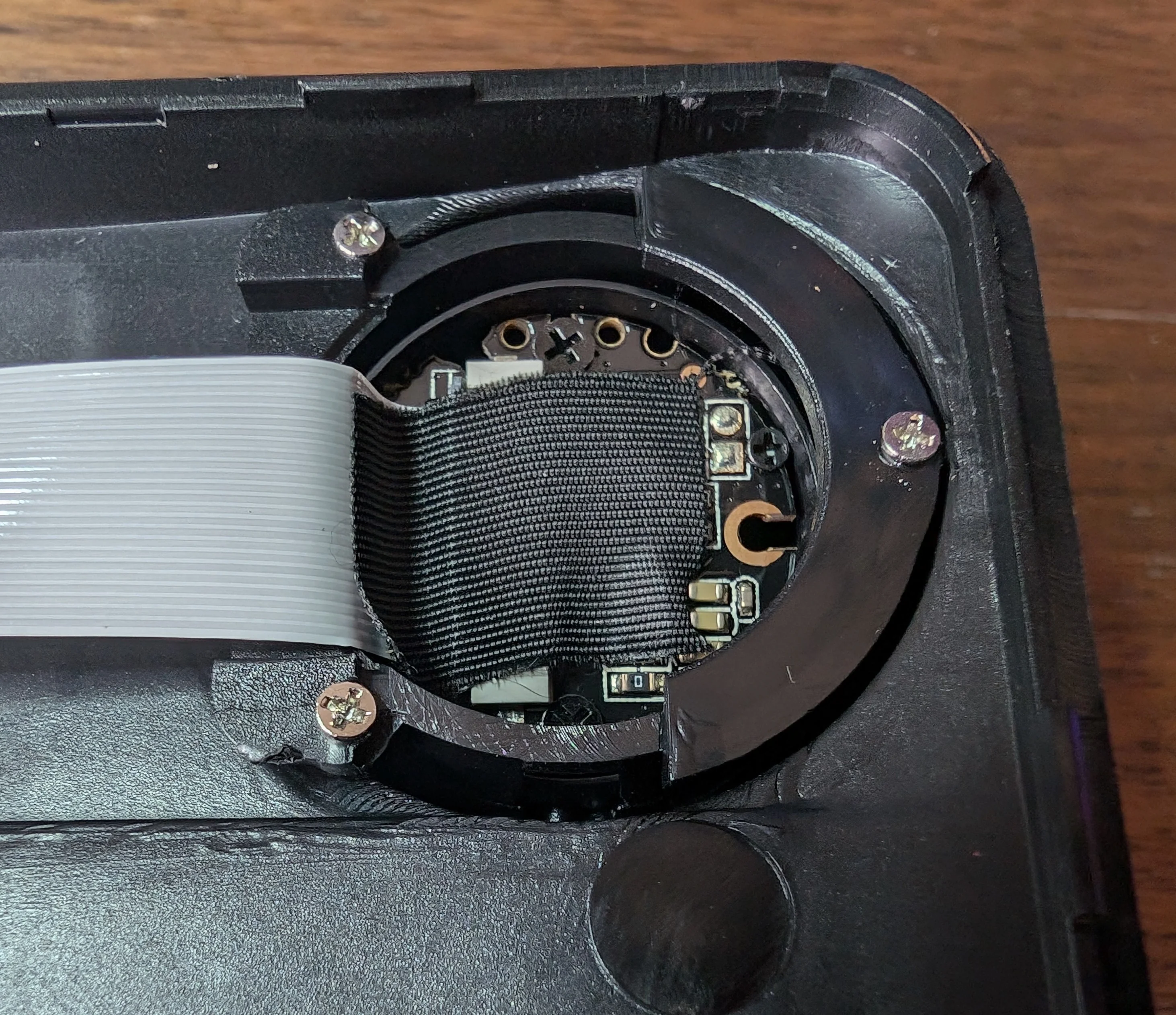
The forward facing camera is in a swivel mount and is highly integrated; there's nothing under that black tape.
PCB Markings
AKA SEO optimization 😉
Main PCB is marked:
77-56V200(20) V3.411
6105
V200-AMWG-V3.411 2019.12.03
And on the rear:
F02Z1B F15Z1B
The main CPU is meant for consumer cameras and is marked:
Hi 3556
RBCV200
CP9881938
1939-CN
The LCD is marked:
XTY TB118-I4018E30A-01
T B118-45a164200402-J
I can’t find a datasheet for what I suspect is the rear-camera processor but it’s marked:
pixelplus
PR2020
S3CWN
KAG2006
Firmware
Just for giggles, I dumped the firmware from the SPI flash to get an idea of what software powers this device.
| |
I did run strings on it and there’s some mildly interesting stuff in there but nothing interesting enough to warrant a deep dive.
binwalk didn’t have any trouble extracting things but I’m not going to spend any time reversing this firmware.
It looked like the usual “bootloader and two identical copies of the application firmware” setup. Taking a look at what I think is the main application:
| |